


Home | Dr. Lenahan | Lab Family Tree | Alumni | People | Research | Publications | Lab Capabilities | Courses | Manuals | Links
Research
Magnetic Resonance in Solid State Electronics
Introduction
Conventional EPR and EDMR are the only techniques with the sensitivity and analytical power to provide definitive (and frequently detailed) information about the atomic scale structure and chemical nature of electrically active defects in electronic materials and devices. EDMR is an EPR based technique in which the EPR measurement is extracted from an “electronic measurement”, that is, a current, a voltage or possibly a capacitance measurement in a fully operational device such as a diode, a bipolar junction transistor, or a MOSFET. These devices are all excellent candidates for quite sensitive EPR measurements based on EDMR. The EDMR technique called spin dependent recombination (SDR) is directly sensitive to electrically active defect centers, at least those with relatively deep levels in almost any solid state device in which can be configured in such a way that one may measure a current significantly influenced by recombination events. Somewhat analogous EDMR measurements could also be made on defects with shallow levels, for example with spin dependent charge pumping. The EDMR technique of spin dependent trap assisted tunneling (SDT) also has great promise for the study of electronic transport in dielectric thin films.
EPR techniques, both conventionally detected ESR and EDMR have a very strong track record in elucidating the atomic scale imperfections involved in many semiconductor materials and devices.
Background: EPR, a Qualitative Introduction
The only technique available with the demonstrated analytical power and the sensitivity to identify electrically active atomic scale defects in semiconductor systems is electron paramagnetic resonance (EPR). The technique is also sometimes called electron spin resonance (ESR). When EPR detection utilizes EDMR, measurements can be made with remarkably high sensitivity in fully processed device structures with the capability to probe many systems on what is truly the nanoscale. Both conventional EPR and EDMR detected EPR studies have identified dozens of trapping defects which affect the electronic response of semiconductor devices. EPR techniques are sensitive to trapping centers with an odd number of electrons in semiconductors and insulators as well as in semiconductor/insulator interfaces. Although a comprehensive explanation of the technique requires a fairly lengthy discussion, the fundamental is simple. A trap which captures a single electron or a hole has an odd number of electrons either before charge capture or after capture. Since EPR techniques are sensitive to sites with an odd number of electrons, it can detect nearly all traps. (Why specify only nearly all? One could imagine a negative U center trap capturing two electrons. It may be possible to trick the negative U center into single electron occupation but …)
In EPR measurements, one places a sample in a large slowly varying magnetic field. A very crude analogy may provide insight: the unpaired electron responds to the magnetic field somewhat like a compass needle responds to the earth’s magnetic field. (The electron is a very small magnet confined to a point, a lot like the compass needle.) This admittedly imperfect but instructive analogy is illustrated in Figure 1. A compass needle will briefly oscillate when the compass is set down. There is a torque on the needle when it’s not pointing north. No torque exists when it points north, but when it swings to north it’s built up some momentum. As it swings past north, the torque builds up again, the process repeats itself till friction damps out the oscillations.
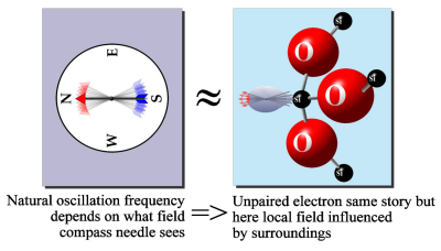 Suppose we were to increase the field experienced by the compass needle; the compass needle oscillation frequency would increase because the torque would increase. It can be shown that the oscillation frequency is proportional to the field the compass needle experiences. The analogy holds, up to a point, for the electron trapped within a defect in a semiconductor or insulator. An increasing magnetic field results in an increasing oscillation frequency. As in the compass needle analogy, the frequency scales with the field which the electron actually experiences. Since the electron in the trap doesn’t experience friction, the oscillations continue forever.
The trick in EPR is the application of a second oscillating field at fixed frequency perpendicular to the large applied field. One typically varies the large field slowly over time. When the fixed frequency matches the electron oscillation frequency, resonance occurs and energy is absorbed by the electron spin. Remember that resonance occurs at a fixed relationship between the microwave frequency and the field the electron actually experiences. That field is, effectively, the sum of the applied magnetic field and the local magnetic field due to the surrounding atoms. If we know the frequency with high precision (we do) and we know the applied field with high precision (we do) we can work backwards to calculate the local field. From knowledge of the local field we can identify the atomic scale structure of the defect site. By measuring the amount of microwave energy absorbed by the sample we can count the number of defects of each type within the sample. The sensitivity of the conventional EPR measurement is about 1010 cm-2. In conventional EPR measurements, the precision in defect counting is about 10% in relative number and somewhat better than a factor of two in absolute number. By comparing EPR measurements (which count defect densities) with electrical measurements (which count various trap densities) one can identify the physical and chemical nature of the defects responsible for traps.
There are unfortunate and obvious limitations of conventional EPR detection in studies of nanoscale semiconductor device problems. Conventional EPR detection is incapable of separating out those defects which play important roles in device operation; the technique is sensitive to all defects within the sample under study, for example every paramagnetic defect in a millimeter square wafer with a “nanoscale’ device mounted on top, EPR detects the defects in the nanoscale structure but also every other paramagnetic defect in the much larger substrate silicon. With a sensitivity limit of around ten billion defects, the conventional measurement is too insensitive to detect defects in most nanoscale structures in which the total number of defects will almost certainly be far less than that sensitivity limit. These problems could be eliminated with electrically detected magnetic resonance (EDMR) typically utilizing spin dependent recombination (SDR). Furthermore SDR/EDMR and other EDMR techniques offer several advantages which conventional EPR could not provide even if its sensitivity and selectivity limitations could be overcome.
To understand the techniques and their capabilities requires a slightly more sophisticated consideration of the physics involved in magnetic resonance.
An Introduction to the Physical Basis for EPR
As mentioned previously, in EPR measurements, the sample under study is exposed to a large slowly varying magnetic field and a microwave frequency magnetic field oriented perpendicularly to the applied field. Usually the measurements are made at an X-band: a microwave frequency υ=9.5 GHz (roughly).
An unpaired electron has two possible orientations in the large applied field and thus two possible orientation dependent energies. (From classical electricity and magnetism, the energy of a magnetic moment µ in a magnetic field H is -µ • H.) Magnetic resonance occurs when the energy difference between the two electron orientations is equal to Planck’s constant, h, times the microwave frequency. For the very simple case of an isolated electron, the resonance requirement may be expressed as
hυ = g0βeH
where g0 = 2.002319 and β is the Bohr magneton, 9.274015×10⁻²⁸ J/G.
The above expression describes the resonance condition for an electron which does not otherwise interact with its surroundings. The structural information provided by EPR is due to deviations from this simple expression. For relatively simple trapping centers, including most or all centers of interest in the proposed study, these deviations are due to spin-orbit coupling and electron–nuclear hyperfine interactions.
Spin-orbit Coupling
 The deviations from the above expression due to spin orbit coupling come about because a charged particle, the electron, is traveling in an electric field due to the nuclear charge. It therefore experiences a magnetic field B=E x v/c2, where E is the electric field, v is the velocity, and c is the speed of light. The spin-orbit interaction may be understood qualitatively (and only qualitatively) in terms of the Bohr picture: an electron moves about the nucleus in a circular orbit. It would appear to an observer on the electron that the positively charged nucleus is in a circular orbit about the electron. (It appears to an unsophisticated observer on earth that the sun is in a circular orbit about the earth.) The nucleus thus generates a local magnetic field which would scale with the electron’s orbital angular momentum, r cross p, and with the nuclear charge. One would thus correctly surmise that spin-orbit coupling interactions increase with increasing atomic number and orbital angular momentum quantum number. This spin-orbit interaction is schematically illustrated in the figure to the left. (Note: figure is intended to provide only a qualitative approximation of reality.)
In solids, the spin-orbit interaction is “quenched” but a second order effect appears from excited states. This effect scales with the applied magnetic field and depends on the orientation of the paramagnetic defect in the applied magnetic field. The spin-orbit coupling may thus be included in the ESR resonance condition by replacing the constant g0 of the simple resonance expression with a second rank tensor gij. The symmetry of this tensor reflects the symmetry of the paramagnetic center. Under some circumstances, the symmetry of the tensor may permit identification of the defect under study.
Electron-Nuclear Hyperfine Interactions
The other important source of deviation from the resonance expression is the hyperfine interaction of the unpaired electron with nearby nuclei. Certain nuclei have magnetic moments; some important examples in semiconductor device materials are 7.8% of germanium nuclei, 73Ge (spin 9/2), 4.7% of silicon nuclei, 29Si (spin ½), almost 100% of hydrogen nuclei, 1H (spin ½), as well as essentially 100% of phosphorous nuclei, 31P (spin ½). The near 100% abundant 14N nucleus has a spin of 1. A spin ½ nucleus has two possible orientations in the large applied field; a spin 1 nucleus three possible orientations. Each nuclear moment orientation corresponds to one local nuclear moment field distribution.
We envision the nuclear moment interacting with an unpaired electron residing in a wave function which is a linear combination of atomic orbitals (LCAOs). For intrinsic defects in, for examples Si, SiGe, GaN, or SiC, or SiO2 and systems based on these materials, the most important cases almost certainly involve s- and p-type wave functions. (For defects involving transition metal impurities, analysis will be somewhat more complicated but the basic principles are the same.)
For a site in which the unpaired electron is reasonably well localized at a single atom, the analysis is particularly simple. To first order we can interpret ESR spectra from such a site in terms of s/p hybridized atomic orbitals localized at that central atom. (The generalization to a defect wave function involving significant sharing by several atoms is very straightforward.)
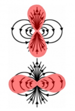
 The electron nuclear hyperfine interaction of an electron in a p orbital is anisotropic: it corresponds to a classical magnetic dipole interaction as schematically illustrated in the figure to the left. The interaction is strongest when the field is parallel to the symmetry axis. The sign of the interaction changes and the magnitude is decreased by one half when the field is perpendicular to the symmetry axis. When the electron and nuclear moments are aligned by a strong magnetic field in the z direction, only the z component of the dipolar field is important, because the interaction energy involves a dot product. -µ • H.
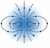
The electron–nuclear hyperfine interaction of an electron in an s orbital is isotropic. This interaction is illustrated in the figure to the right. The figure shows why the interaction is isotropic. The spherical symmetry of the orbital results in zero interaction with this field except for a spherical region about the nucleus with a radius of an imaginary current loop generating the nuclear moment’s field. Since the s orbital has a nonzero probability density at the nucleus, a large isotropic interaction results.
Spin Dependent Recombination (SDR):
 Spin dependent recombination (SDR) is an EPR technique in which one can make EPR measurements on quite small fully processed devices, including devices in integrated circuits. In SDR, the spin dependent nature of recombination events is exploited so that one may observe EPR through measurement of recombination currents. A (not quite right but instructive) explanation of SDR, first proposed by Lepine, is sufficient for a qualitative understanding. The Lepine model combines the Shockley-Read-Hall (SRH) recombination model and the Pauli Exclusion Principle.
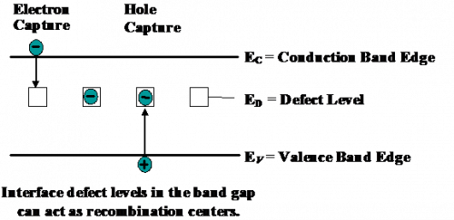
 In the SRH model, recombination of electrons and holes takes place through deep level defects in the semiconductor bandgap. An electron is trapped at a deep level defect, then a hole is trapped at the same deep level defect. (The sequence could obviously be reversed, with a hole being trapped first at a deep level defect, then an electron.) This process is illustrated in figure to the right.
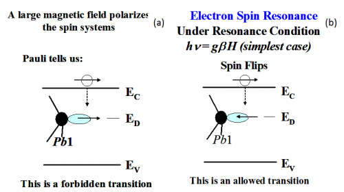
Suppose that the deep level defect is a “dangling bond.” The dangling bond has an unpaired electron when it is electrically neutral. In SDR, the semiconductor device is placed in a strong magnetic field which polarizes the spins of the dangling bond electrons as well as the conduction electrons and holes. (That is, the electron spins tend to orient with the applied magnetic field.) The SRH recombination process begins with the electron capture (or hole capture) at the deep level site. If both the dangling bond and conduction electrons have the same spin orientation, the conduction electron cannot be captured at the site because two electrons may not occupy the same orbital with the same spin quantum number. Thus, placing the semiconductor sample in the magnetic field reduces the average trap capture cross section of the traps. In EPR, electron spins are “flipped” from one spin orientation to the other when the resonance condition is satisfied. The spin flipping at the trap site increases the probability of oppositely oriented traps and conduction electron spins, allowing the trapping event and recombination. This process increases the recombination current. This process is illustrated in the figure to the left.
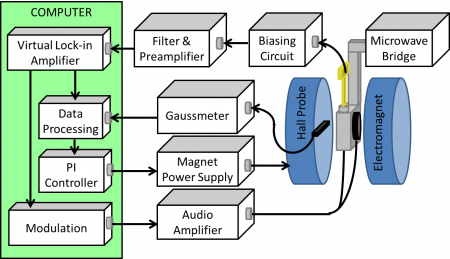 Thus, if a semiconductor device is placed in a strong slowly varying magnetic field and microwave radiation, the recombination current will increase when the applied magnetic field and microwave frequency satisfy the resonance condition. The device current plotted versus magnetic field will have the same pattern as that of the ESR spectrum of the defect under study. An SDR spectrometer is schematically illustrated in the figure to the right. Although the simple model discussed herein provides a qualitative understanding of SDR, a much more accurate SDR developed by Kaplan et. al (1978) provides the foundation for the present day understanding of the phenomenon.
In SDR measurements, a device needs to be configured in such a way that the measured current would be strongly influenced by recombination events. In the case of MOSFETs, one may do this by configuring the device as a gated diode; connect the source to drain together and apply a modest bias across the source-drain to substrate junction. With modest forward bias, the current will be dominated by recombination. If the gate is biased so that the semiconductor/ insulator interface quasi-Fermi levels of the electrons and holes are symmetric about the intrinsic level, equal numbers of electrons and holes will be present at that interface, usually the location of the great majority of electrically active (deep level) defects, the recombination centers. Placing equal numbers of electrons and holes at the primary location of recombination centers will yield a maximum value in recombination current. With such biasing conditions, one then applies the large slowly varying magnetic field and microwave radiation required for EPR to take place. The recombination current will be altered by SDR/EDMR yielding essentially the same field- frequency response as the conventional EPR spectrum.
Qualitative Introduction to Electron Paramagnetic Resonance
Physical Basis for EPR
Spin Dependent Recombination
References